鐣欒█璇环
鐣欒█璇环


铏氭嫙鍙峰皢鍦180绉掑悗澶辨晥
浣跨敤寰俊鎵爜鎷ㄥ彿
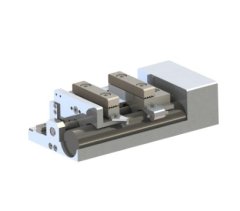
纭掑寲閿岋紙ZnSe锛堻/span>ATR妫遍暅
ZnSe鍦ㄧ孩澶栧厓鍣ㄤ欢绐楃墖閫忛暅浠ュ強鍏夎氨鍒嗘瀽ATR妫遍暅棰嗗煙鏈夌潃骞挎硾鐨勫簲鐢ㄣ€傜鍖栭攲(Zinc Selenide)瀵逛簬CO2婵€鍏夊櫒鐨勫厓鍣ㄤ欢涔熸槸涓€绉嶈壇濂界殑閫夋嫨銆傚湪浜屾哀鍖栫⒊婵€鍏夊櫒宸ヤ綔鐨勬尝娈袋/span>10.6 microns闄勮繎鏈夌潃鑹ソ鐨勯€忓皠鐜囥€傜鍖栭攲鏉愭枡鏄竴绉嶉粍鑹查€忔槑鐨勫鏅舵潗鏂橖/span>锛缁撴櫠棰楃矑澶у皬绾︿负70μm锛閫忓厜鑼冨洿0.5-15μm銆傜敱鍖栧姘旂浉娌夌Н(CVD)鏂规硶鍚堟垚鐨勫熀鏈笉瀛樺湪鏉傝川鍚告敹锛鏁e皠鎹熷け鏋佷綆銆傜敱浜庡10.6μm娉㈤暱鍏夌殑鍚告敹寰堝皬锛鍥犳鎴愪负鍒朵綔楂樺姛鐜嘃/span>CO2婵€鍏夊櫒绯荤粺涓厜瀛﹀櫒浠剁殑**鏉愭枡銆侟/span>姝ゅ鍦ㄥ叾鏁翠釜閫忓厜娉㈡鍐匋/span>锛涔熸槸鍦ㄤ笉鍚屽厜瀛︾郴缁熶腑鎵€鏅亶浣跨敤鐨勬潗鏂欍€侟/span>
纭掑寲閿屾潗鏂欏鐑啿鍑诲叿鏈夊緢楂樼殑鎵垮彈鑳藉姏锛浣垮畠鎴愪负楂樺姛鐜嘃/span>CO2婵€鍏夊櫒绯荤粺涓殑**鍏夊鏉愭枡銆傜‖搴﹀彧鏄鍏夎氨绾?/span>ZnS鐨凕/span>2/3锛鏉愯川杈冭蒋鏄撲骇鐢熷垝鐥旤/span>锛鑰屼笖鏉愭枡鎶樺皠鐜囪緝澶?/span>锛鎵€浠ラ渶瑕佸湪鍏惰〃闈㈤晙鍒堕珮纭害鍑忓弽灏勮啘鏉ュ姞浠ヤ繚鎶ゅ苟鑾峰緱杈冮珮鐨勯€忚繃鐜囥€傚湪鍏跺父鐢ㄥ厜璋辫寖鍥村唴锛鏁e皠寰堜綆銆傚湪鐢ㄥ仛楂樺姛鐜囨縺鍏夊櫒浠舵椂锛闇€瑕佷弗鏍兼帶鍒舵潗鏂欑殑浣撳惛鏀跺拰鍐呴儴缁撴瀯缂洪櫡锛骞堕噰鐢?灏忕牬鍧忕▼搴︾殑鎶涘厜鎶€鏈拰**鍏夊璐ㄩ噺鐨勯晙鑶滃伐鑹恒€侟/span>
骞挎硾搴旂敤浜庢縺鍏堻/span>锛孅span>鍖诲锛屽ぉ鏂囧鍜岀孩澶栧瑙嗙瓑棰嗗煙涓€侟/span>
鍙傛暟璇︾粏淇℃伅锛欬/span>
閫忓皠娉㈡鑼冨洿: |
0.6 to 21.0um |
鎶樺皠鐜囷細 |
2.4028 at 10.6um |
鍙嶅皠鎹熻€楋細 |
29.1% at 10.6um (2 surfaces) |
鍚告敹绯绘暟锛欬/span> |
0.0005 cm-1at 10.6um |
鍚告敹宄帮細 |
45.7um |
dn/dT : |
+61 x 10-6/鈩傸/span>at 10.6um at 298K |
dn/du= 0 : |
5.5um |
瀵嗗害锛欬/span> |
5.27 g/cc |
鐔旂偣锛欬/span> |
1525鈩傸/span>(see notes below) |
瀵肩儹绯绘暟锛欬/span> |
18 W m-1K-1at 298K |
鐑啫鑳€锛欬/span> |
7.1 x 10⁻⁶/鈩傸/span>at 273K |
纭害: |
Knoop 120 with 50g indenter |
姣旂儹瀹归噺 : |
339 J Kg-1K-1 |
Dielectric Constant : |
n/a |
Youngs Modulus (E) : |
67.2 GPa |
Shear Modulus (G) : |
n/a |
Bulk Modulus (K) : |
40 GPa |
寮规€х郴鏁?/span>: |
Not Available |
Apparent Elastic Limit : |
55.1 MPa (8000 psi) |
娉婃澗姣 : |
0.28 |
Solubility : |
0.001g/100g water |
Molecular Weight : |
144.33 |
Class/Structure : |
HIP polycrystalline cubic锛 ZnS锛 F43m |
No = Ordinary Ray
μm |
No |
μm |
No |
μm |
No |
0.54 |
2.6754 |
0.58 |
2.6312 |
0.62 |
2.5994 |
0.66 |
2.5755 |
0.7 |
2.5568 |
0.74 |
2.5418 |
0.78 |
2.5295 |
0.82 |
2.5193 |
0.86 |
2.5107 |
0.90 |
2.5034 |
0.94 |
2.4971 |
0.98 |
2.4916 |
1.0 |
2.4892 |
1.4 |
2.4609 |
1.8 |
2.4496 |
2.2 |
2.4437 |
2.6 |
2.4401 |
3.0 |
2.4376 |
3.4 |
2.4356 |
3.8 |
2.4339 |
4.2 |
2.4324 |
4.6 |
2.4309 |
5.0 |
2.4295 |
5.4 |
2.4281 |
5.8 |
2.4266 |
6.2 |
2.4251 |
6.6 |
2.4235 |
7.0 |
2.4218 |
7.4 |
2.4201 |
7.8 |
2.4183 |
8.2 |
2.4163 |
8.6 |
2.4143 |
9.0 |
2.4122 |
9.4 |
2.4100 |
9.8 |
2.4077 |
10.2 |
2.4053 |
10.6 |
2.4028 |
11.0 |
2.4001 |
11.4 |
2.3974 |
11.8 |
2.3945 |
12.2 |
2.3915 |
12.6 |
2.3883 |
13.0 |
2.3850 |
13.4 |
2.3816 |
13.8 |
2.3781 |
14.2 |
2.3744 |
14.6 |
2.3705 |
15.0 |
2.3665 |
15.4 |
2.3623 |
15.8 |
2.3579 |
16.2 |
2.3534 |
16.6 |
2.3487 |
17.0 |
2.3438 |
17.4 |
2.3387 |
17.8 |
2.3333 |
18.2 |
2.3278 |
璁㈣喘淇℃伅锛欬/span>
浜у搧鍨嬪彿 |
瑙勬牸 |
澶栧舰 |
鏉愭枡绛夌骇 |
ZNSEPRISM42-14-2-45 |
42 x 14 x 2mm 45° ATR |
姊舰 |
IR Polished |
ZNSEPRISM50-20-2-30 |
50 x 20 x 2mm 30° ATR |
姊舰 |
IR Polished |
ZNSEPRISM52-20-2-45 |
52 x 20 x 2mm 45° ATR |
姊舰 |
IR Polished |
ZNSEPRISM52-20-2-60 |
52 x 20 x 2mm 60° ATR |
姊舰 |
IR Polished |
ZNSEPRISM60-12-4-45P |
60 x 12 x 4mm 45° ATR |
姊舰 |
IR Polished |
ZNSEPRISM60-15-3-30 |
60 x 15 x 3mm 30° ATR |
姊舰 |
IR Polished |
ZNSEPRISM60-15-3-45 |
60 x 15 x 3mm 45° ATR |
姊舰 |
IR Polished |
ZNSEPRISM60-15-3-60 |
60 x 15 x 3mm 60° ATR |
姊舰 |
IR Polished |
ZNSEPRISM68-10-6-45 |
68 x 10 x 6mm 45° ATR |
姊舰 |
IR Polished |
绀轰緥锛欬/span>ZNSEPRISM50-20-2-30
鍏充簬鏅朵綋鍒囧壊锛欬/span>
During Chemical Vapour Deposition the small crystallite grains align with thedirection of growth锛 and are
normal to the thickness of the sheet produced. For windows of normal thickness and aspect ratios the alignmentof the grain therefore is rarely a problem as they are cut from the grown sheet such that within an optical windowthe grains align perpendicular to the surfaces. This is optimum orientation for lowest internal absorption andscatter.
With prisms锛 the cutting direction requires more consideration. It isrecommended that the thickness of the stripmaterial corresponds to the apex height of the prism. This ensures optimum crystallite orientation for most usual
prism applications.
For typical 45° prisms the most obvious use of material is shown in (A) but it
should be noted that this is not the optimum orientation.
The best choice is (B) and it also permitsa higher limit on prism size orconverselyallows thinner stock to be used. There iswaste at the ends of the strip but this issmall and so it may not be quite aseconomic as (A).
Cutting in direction (C) where the entire light beam runs at 90° to the grain
structure should be avoided completely if at all possible.Note that maximum available thickness of ZnSe and ZnS (FLIR) is approximately 60mm. Maximum availablethickness of ZnS Cleartran is approximately 30mm
鏆傛棤鏁版嵁锛
 纭掑寲閿岋紙ZnSe锛堿TR妫遍暅鐨勫伐浣滃師鐞嗕粙缁嶏紵纭掑寲閿岋紙ZnSe锛堿TR妫遍暅鐨勪娇鐢ㄦ柟娉曪紵纭掑寲閿岋紙ZnSe锛堿TR妫遍暅澶氬皯閽变竴鍙帮紵纭掑寲閿岋紙ZnSe锛堿TR妫遍暅浣跨敤鐨勬敞鎰忎簨椤更/li>纭掑寲閿岋紙ZnSe锛堿TR妫遍暅鐨勮鏄庝功鏈夊悧锛烖/li>纭掑寲閿岋紙ZnSe锛堿TR妫遍暅鐨勬搷浣滆绋嬫湁鍚楋紵纭掑寲閿岋紙ZnSe锛堿TR妫遍暅鐨勬姤浠峰惈绁ㄥ惈杩愯垂鍚楋紵纭掑寲閿岋紙ZnSe锛堿TR妫遍暅鏈夌幇璐у悧锛烖/li>纭掑寲閿岋紙ZnSe锛堿TR妫遍暅鍖呭畨瑁呭悧锛烖/li>


 鎵嬫満鐗堬細