ç™»ه½•

- APP
ن¸ه›½ç²‰ن½“网و¬¢è؟ژو‚¨ï¼?/div>
- 粉ن؛«é€™ü/a>
- ه¹؟ه‘ٹوœچهٹ،
ه¾®ن؟،

 ه…³و³¨ه¾®ن؟،ه…¬ن¼—هڈ¶ü/span>
- ن¸ه›½ç²‰ن½“ç½گü/a>
 移هٹ¨ç«?/p>
 m.cnpowder.com.cn
ç™»ه½•
ه¾®ن؟،

 ه…³و³¨ه¾®ن؟،ه…¬ن¼—هڈ¶ü/span>
![]() 移هٹ¨ç«?/p>
移هٹ¨ç«?/p>
 m.cnpowder.com.cn


هڈ‚考ن»·و »ü/p>é¢è®®
ه‹هڈ·
ه“پ牌
ن؛§هœ°
ه¾·ه›½و ·وœ¬
وڑ‚و—ن¼ڑه‘ک
|ç¬?ه¹³ü/p>|
ç”ںن؛§ه•…ü/p>
![]() ه·¥ه•†ه·²و ¸ه®ü/p>
ه·¥ه•†ه·²و ¸ه®ü/p>
 留言询ن»·
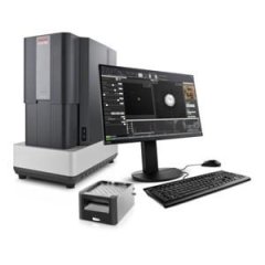
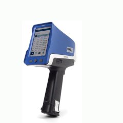
看ن؛†è¶…é«کهˆ†è¾¨و•£ه°„ه¼ڈè؟‘هœ؛ه…‰ه¦وک¾ه¾®é•œ-neaSNOMçڑ„用وˆ·هڈˆçœ‹ن؛†
留言询ن»·


è™ڑو‹ںهڈ·ه°†هœ180秒هگژه¤±و•ˆ
ن½؟用ه¾®ن؟،و‰«ç پو‹¨هڈ·
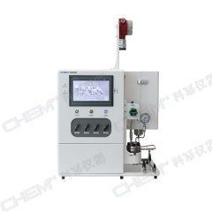
超é«کهˆ†è¾¨و•£ه°„ه¼ڈè؟‘هœ؛ه…‰ه¦وک¾ه¾®é•œ - neaSNOM
ن؛§ه“پ简ن»‹ï¼ڑ
neaSNOMوک¯ه¾·ه›½neaspecه…¬هڈ¸وژ¨ه‡؛çڑ„第ن¸‰ن»£و•£ه°„ه¼ڈè؟‘هœ؛ه…‰ه¦وک¾ه¾®é•œï¼ˆç®€ç§°s-SNOM),ه…¶é‡‡ç”¨ن؛†**هŒ–çڑ„و•£ه°„ه¼ڈو ¸ه؟ƒè®¾è®،وٹ€وœ¯ï¼Œوپه¤§çڑ„وڈگé«کن؛†ه…‰ه¦هˆ†è¾¨çژ‡ï¼Œه¹¶ن¸”ن¸چن¾èµ–ن؛ژه…¥ه°„و؟€ه…‰çڑ„و³¢é•؟,能ه¤ںهœ¨هڈ¯è§پم€پç؛¢ه¤–ه’Œه¤ھ赫ه…¹ه…‰è°±èŒƒه›´ه†…,وڈگن¾›ن¼کن؛?0nmç©؛é—´هˆ†è¾¨çژ‡çڑ„ه…‰è°±ه’Œè؟‘هœ؛ه…‰ه¦ه›¾هƒڈم€‚ç”±ن؛ژه…¶é«که؛¦çڑ„هڈ¯é و€§ه’Œهڈ¯é‡چه¤چو€§ï¼ŒneaSNOMن¸ڑه·²وˆگن¸؛ç؛³ç±³ه…‰ه¦é¢†هںںçƒç‚¹ç ”究و–¹هگ‘çڑ?*ç§‘ç ”è®¾ه¤‡ï¼Œهœ¨ç‰ç¦»هں؛ه…ƒم€پç؛³ç±³FTIRه’Œه¤ھ赫ه…¹ç‰ن¼—ه¤ڑç ”ç©¶و–¹هگ‘ه¾—هˆ°ن؛†è®¸ه¤ڑé‡چè¦پç§‘ç ”وˆگوœم€پü/span>
*è؟‘,neaspecه…¬هڈ¸وˆگهٹںه¼€هڈ‘ن؛†هڈ¯è§پ至ه¤ھ赫ه…¹é«کهˆ†è¾¨ه…‰è°±ه’Œوˆگهƒڈ综هگˆç³»ç»ں,ه°†ن¸ٹè؟°s-SNOMهٹں能ن¸ژç؛³ç±³ç؛¢ه¤–(FTIR)م€پé’ˆه°–ه¢ه¼؛و‹‰و›¼ï¼ˆTERS)م€پ超ه؟«ه…‰è°±ï¼ˆultrafast)ه’Œه¤ھ赫ه…¹ه…‰è°±ï¼ˆTHz)è؟›è،Œèپ”用,هڈ¯ن»¥ن¸؛ه¹؟ه¤§ç§‘ه¦ه·¥ن½œè€…هœ¨ç‰ç¦»هگو؟€ه…‚ü/span>م€?/span>ن؛Œç»´وگو–™ه£°هگوپهŒ–م€?/span>هچٹه¯¼ن½“è½½وµپهگوµ“ه؛¦هˆ†ه¸ƒم€?/span>ç”ں物وگو–™ç؛¢ه¤–è،¨ه¾پم€?/span>电هگو؟€هڈ‘هڈٹè،°ه‡ڈè؟‡ç¨‹ç‰çڑ„ç ”ç©¶ن¸ٹوڈگن¾›ç›¸ه…³و”¯وŒپم€پü/span>
وٹ€وœ¯ç‰¹ç‚¹ه’Œن¼کهٹ؟ï¼™ü/span>
neaSNOMوک¯ç›®ه‰چن¸–ç•Œن¸ٹéه¸¸وˆگç†ںçڑƒü/strong>s-SNOMن؛§ه“پ **ن؟وٹ¤çڑ„و•£ه°„ه¼ڈè؟‘هœ؛ه…‰ه¦وµ‹é‡ڈوٹ€وœ?/strong> —独وœ‰çڑ„وپé«ک10 nmç©؛é—´هˆ†è¾¨çژ†ü/span> **çڑ„é«کéک¶è§£è°ƒèƒŒو™¯هژ‹ç¼©وٹ€وœ?/strong> —هœ¨èژ·ه¾—10nmç©؛é—´هˆ†è¾¨çژ‡çڑ„هگŒو—¶ن؟وŒپوپé«کçڑ„ن؟،ه™ھو¯” ن¸’ü/strong>هˆ©ن؟وٹ¤çڑ„ه¹²و¶‰ه¼ڈè؟‘هœ؛ن؟،هڈ·وژ¢وµ‹هچ•ه…‚ü/strong>?**çڑ„èµه¤–ه·®ه¹²و¶‰ه¼ڈوژ¢وµ‹وٹ€وœ?/strong> —能ه¤ںèژ·ه¾—ه¯¹è؟‘هœ؛ن؟،هڈ·ه¼؛ه؛¦ه’Œç›¸ن½چçڑ„هگŒو¥وˆگهƒڈ |
**ن؟وٹ¤çڑ„هڈچه°„ه¼ڈه…‰ه¦ç³»ç»ں —用ن؛ژه®½و³¢é•؟范ه›´çڑ„ه…‰و؛گï¼ڑهڈ¯è§پم€پç؛¢ه¤–ن»¥è‡³ه¤ھ赫ه…¹ é«ک稳ه®ڑو€§çڑ„AFMç³»ç»ں —هگŒو—¶ن¼کهŒ–ن؛†ç؛³ç±³ه°؛ه؛¦ن¸‹ه…‰ه¦وµ‹é‡ژü/span> هڈŒه…‰وںè®¾è® ü/strong> —وپé«کçڑ„ه…‰ه¦وژ¥ه…¥è§’ï¼ڑو°´ه¹³و–¹هگ‘180،م,ه‚ç›´و–¹هگ?0،م و“چن½œه’Œو ·ه“په‡†ه¤‡ç®€هچ”ü/strong> —ن»…需è¦په¸¸è§„çڑ„AFMو ·ه“په‡†ه¤‡è؟‡ç¨‹ |
é‡چè¦په؛”用领هںںï¼™ü/strong>
部هˆ†هڈ‘è،¨و–‡ç« ï¼™ü/span>
Science (2017)doi:10.1126/science.aan2735 |
Tuning quantum nonlocal effects in graphene plasmonics |
Nature Nanotechnology (2017)doi:10.1038/nnano.2016.185 |
Acoustic terahertz graphene plasmons revealed by photocurrent nanoscopy |
Nature Photonics (2017)doi:10.1038/nphoton.2017.65 |
Imaging exciton–polariton transport in MoSe2 waveguides |
Nature Materials(2016)doi:10.1038/nnano.2016.185 |
Acoustic terahertz graphene plasmons revealed by photocurrent nanoscopy |
Nature Materials(2016)doi:10.1038/nmat4755 |
Thermoelectric detection and imaging of propagating graphene plasmons |
ه›½ه†…用وˆ·هڈ‘è،¨و–‡ç« ï¼™ü/span>
Nat. Commun.8ï¼ 15561(2017) |
Imaging metal-like monoclinic phase stabilized by surface coordination effect in vanadium dioxide nanobeam |
Adv. Mater.29ï¼ 1606370 (2017) |
The Light-Induced Field-Effect Solar Cell Concept –Perovskite Nanoparticle Coating Introduces Polarization Enhancing Silicon Cell Efficiency |
Light- Sci & Appl6ï¼ 204(2017) |
Effects of edge on graphene plasmons as revealed by infrared nanoimaging |
Light- Sci & Appl+ü/strong>ن¸ه±±ه¤§ه¦accepted(2017) |
Tailoring of electromagnetic field localizations by two-dimensional graphene nanostructures |
Nanoscale9ï¼ 208(2017) |
Study of graphene plasmons in graphene–MoS2 heterostructures for optoelectronic integrated devices |
Nano-Micro Lett.9ï¼?(2017) |
Molybdenum Nanoscrews: A Novel Non-coinage-Metal Substrate for Surface-Enhanced Raman Scattering |
J. Phys. D: Appl. Phys.50ï¼ 094002(2017) |
High performance photodetector based on 2D CH3NH3PbI3 perovskite nanosheets |
ACS Sens.2ï¼ 386(2017) |
Flexibleï¼ Transparentï¼ and Free-Standing Silicon Nanowire SERS Platform for in Situ Food Inspection |
Semiconductor Sci. and Tech.32ï¼?74003 (2017) |
PbI2 platelets for inverted planar organolead Halide Perovskite solar cells via ultrasonic spray deposition |
部هˆ†ç”¨وˆ·ه¥½è¯„ن¸ژهˆ—è،¨ï¼ˆوژ’هگچن¸چهˆ†ه…ˆهگژ(ü/span>
neaspecه…¬هڈ¸ن؛§ه“پن»¥ه…¶ç¨³ه®ڑçڑ„و€§èƒ½م€پوپé«کçڑ„ç©؛é—´هˆ†è¾¨çژ‡ه’Œè‰¯ه¥½çڑ„用وˆ·ن½“éھŒï¼Œه¾—هˆ°ن؛†ه›½ه†…ه¤–ن¼—ه¤ڑ科ه¦ه®¶çڑ„认هڈ¯ه’Œè‚¯ه®?.....
Prof. Dmitri Basov ç¾ژه›½ هٹ ه·ه¤§ه¦ University of California San Diego |
"The neaSNOM microscope with it’s imaging and nano-FTIR mode is the most useful research instrument in yearsï¼ bringing genuinely new insights." |
|
Dr. Jaroslaw Syzdekç¾ژه›½ هٹ³ن¼¦و–¯ن¼¯ه…‹هˆ©ه›½ه®¶ه®éھŒه®£ü/strong> Lawrence Berkeley National Laboratory |
"We were looking for a flexible research tool capable of characterizing our energy storage materials at the nanoscale. neaSNOM proofed to be the system with the highest spatial resolution in infrared imaging and spectroscopy and brings us substantial new insights for our research“ü/span> |
|
陈焕هگ و•™وژˆن¸ه±±ه¤§ه¦Sun Yat-sen University |
"The neaSNOM microscope boosted my research in plasmonic properties of noble metal nanocrystalsï¼ optical resonances of dielectric nanostructuresï¼ and plasmon polaritons of graphene-like two dimensional nanomaterials." |
|
Prof. Rainer HillenbrandResearch Center Co-Founder and Scientific Advisor |
"After many years of research and development in near-field microscopyï¼ we finally made our dream come true to perform infrared imaging & spectroscopy at the nanoscale. With neaSNOM we can additionally realize Ramanï¼ fluorescence and non-linear nano-spectroscopy." |
|
Dr. Dangyuan Lei The Hong Kong Polytechnic University Department of Applied Physics Hong Kong |
"We propose to establish a complete set of nano-FTIR and scattering-type SNOM in order to stay competitive in nanophotonics research as well as to maintain our state-of-the-art design and fabrication of novel nanomaterials. Only because of the unique technology from neaspec we were able to win this desirable university grant." |
|
Prof. Dan Mittleman Brown University School of Engineering USA |
"The neaSNOM near-field microscope and it’s user-friendly software offer us an incredible flexibility for the realization of our unique experiments †without compromises in robustnessï¼ handling and ease-of-use." |
|
Dr. Raul Freitas Centro Nacional de Pesquisa em Energia e Materiais (CNPEM) Laborat¨®rio Nacional de Luz S¨ھncrotron (LNLS) Brazil |
"The great stability and robustness of the neaSNOM are key features for serving our diverse user’s demands. The neaSCAN software is user-friendly and intuitive allowing fresh users to quickly start measuring." |
|
Prof. Dr. Rupert Huber University of Regensburg Department of Phyics Germany |
"The unique dual beam-path design of the neaSNOM near-field microscope makes neaspec the natural choice for ultrafast spectroscopy at the nanoscale." |
ه›½ه†…部هˆ†ç”¨وˆ·ï¼ˆوژ’هگچن¸چهˆ†ه…ˆهگژ)9ü/span>
و¸…هچژه¤§ه¦ |
ن¸œهچ—ه¤§ه¦ |
ن¸ç§‘院物çگ†و‰€ |
ن¸ç§‘院ن¸ٹوµ·وٹ€ç‰©و‰€ |
香و¸¯çگ†ه·¥ه¤§ه¦ |
ن¸ه±±ه¤§ه¦ |
è‹ڈه·ه¤§ه¦ |
ن¸ç§‘院ه¤§è؟هŒ–物و‰€ |
ن¸ه›½ç§‘ه¦وٹ€وœ¯ه¤§ه?/span> |
首都ه¸ˆèŒƒه¤§ه¦ |
ه››ه·ه¤§ه¦ |
هچ—ه¼€ه¤§ه¦ |
ه›½ه®¶ç؛³ç±³ç§‘ه¦ن¸ه؟ƒ |
ن¸ç§‘院وˆگ都ه…‰ç”µو‰€ |
هŒ—ن؛¬ه¸ˆèŒƒه¤§ه¦ |
وڑ‚و— و•°وچ®ï¼
 超é«کهˆ†è¾¨و•£ه°„ه¼ڈè؟‘هœ؛ه…‰ه¦وک¾ه¾®é•œ-neaSNOMçڑ„ه·¥ن½œهژںçگ†ن»‹ç»چï¼ں超é«کهˆ†è¾¨و•£ه°„ه¼ڈè؟‘هœ؛ه…‰ه¦وک¾ه¾®é•œ-neaSNOMçڑ„ن½؟用و–¹و³•ï¼ں超é«کهˆ†è¾¨و•£ه°„ه¼ڈè؟‘هœ؛ه…‰ه¦وک¾ه¾®é•œ-neaSNOMه¤ڑه°‘é’±ن¸€هڈ°ï¼ں超é«کهˆ†è¾¨و•£ه°„ه¼ڈè؟‘هœ؛ه…‰ه¦وک¾ه¾®é•œ-neaSNOMن½؟用çڑ„و³¨و„ڈن؛‹é،¸ü/li>超é«کهˆ†è¾¨و•£ه°„ه¼ڈè؟‘هœ؛ه…‰ه¦وک¾ه¾®é•œ-neaSNOMçڑ„说وکژن¹¦وœ‰هگ—ï¼ü/li>超é«کهˆ†è¾¨و•£ه°„ه¼ڈè؟‘هœ؛ه…‰ه¦وک¾ه¾®é•œ-neaSNOMçڑ„و“چن½œè§„程وœ‰هگ—ï¼ں超é«کهˆ†è¾¨و•£ه°„ه¼ڈè؟‘هœ؛ه…‰ه¦وک¾ه¾®é•œ-neaSNOMçڑ„وٹ¥ن»·هگ«ç¥¨هگ«è؟گè´¹هگ—ï¼ں超é«کهˆ†è¾¨و•£ه°„ه¼ڈè؟‘هœ؛ه…‰ه¦وک¾ه¾®é•œ-neaSNOMوœ‰çژ°è´§هگ—ï¼ü/li>超é«کهˆ†è¾¨و•£ه°„ه¼ڈè؟‘هœ؛ه…‰ه¦وک¾ه¾®é•œ-neaSNOMهŒ…ه®‰è£…هگ—ï¼ü/li>
 و‰‹وœ؛版ï¼ڑ